


This project describes how to
design a custom inclinometer subsystem capable of measuring angles
accurately down to three-thousandths of a degree.
This project creates an inclinometer subsystem that might be used in precision instruments. With this design, I can record an angle down to one-hundredth of a degree and know it’s accurate. I can look at it down to one-thousandth of a degree and know with 99.999999% confidence that it is within three-thousandths of a degree.
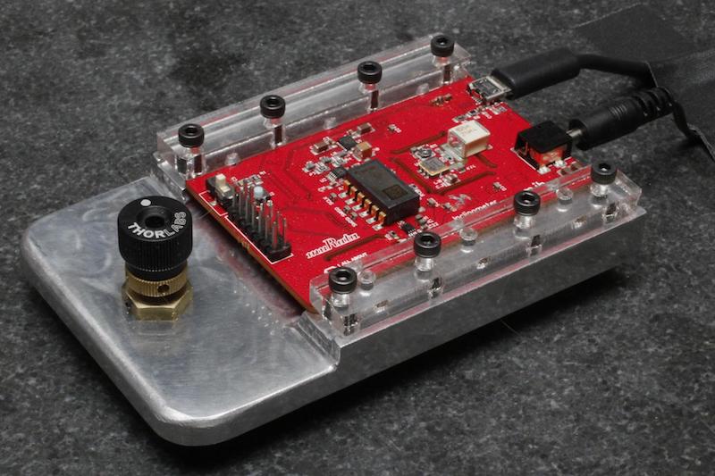
The final build of the project
This project creates a 1-axis digital and mechanical inclinometer for use in scientific instruments or machinery. The circuit board utilizes ICs from a variety of manufacturers and demonstrates several different techniques that you might incorporate into your designs.

A very simple block diagram of the project
This article is the first in a series that shows some of the mechanical and electrical considerations needed to create a precision inclinometer circuit using the muRata SCA103T-D04, a ±15° MEMS-based inclinometer IC. Future articles will cover the schematic design, PCB layout considerations, and analysis of the device's operation in more detail.
1. Choosing Components
Here's a simplified BOM of the major components you'll need to copy my design:- SCA103T-D04 ±15° inclinometer
- MSP430 microcontroller
- AD8244 unity-gain amplifier
- LTC2380IDE SAR ADC
- LT1027LS8 precision voltage reference
- CP2102N UART-to-USB converter
How Does the Design Work?
The design is centered around the SCA103T-D04 ±15°
inclinometer IC. In the interest of disclosure, let me mention
that muRata sent me this inclinometer for free for the purposes of this
article.
Regrettably, I learned (too late) that this particular
component is set to be discontinued. The muRata website currently states
that the SCA103T-D04's "Last Time Buy Date" is 6/15/2019.
Sensor output from the inclinometer is sent through an Analog Devices AD8244 unity-gain amplifier to an LTC2380IDE successive approximation register (SAR) analog-to-digital converter (ADC) from Linear Technology (now part of Analog Devices). I
chose a 24-bit SAR ADC instead of a 16-bit device, knowing full well
that it is physically and practically impossible to resolve down to
0.00000001°. I made my target 17-18 bits, or 0.0001°. This is a somewhat
expensive choice, so if anyone wants to re-create this design later
with a 16-bit ADC, you will be glad to know that I chose one with an
available pin-compatible 16-bit version.
The ADC value is read by the TI MSP430 microcontroller. TI’s MSP430 microcontrollers have been my MCUs of choice for the last several projects. I could have chosen the MSP430FR2433 to have access to additional GPIO lines, but no other pins were required for this project. The MSP430FR2633 has capacitive touch pin capability that would allow an external calibration button to be implemented on a future control board.
That value is then passed to the Silicon Labs CP2102N UART-to-USB converter.
About the Inclinometer
The muRata SCA103T-D04
±15° analog high-performance differential 1-axis inclinometer has an
analog resolution of 0.001° (16-bit), with 0.0004°/√Hz output noise
density and an offset temperature dependency of ±0.002°/°C.

The SCA103T-D04. Image from muRata
An
integrated 11-bit ADC provides direct digital conversion for output
through the SPI pins. Each internal sensing element provides
single-ended output in the range of 0.5-4.5VDC, with 0-0.5VDC
and 4.5-5.0VDC reserved to indicate an error condition.

A functional block diagram of the SCA103T-D04, from the datasheet
Inside
the IC are two identical accelerometers arranged along the same axis
and pointing in opposite directions. The outputs are meant to feed a
differential amplifier or differential-input ADC. This differential measurement technique helps to reduce noise and removes common-mode measurement errors.
muRata’s
datasheet states that the device is capable of discerning angular
displacement with a resolution of 0.001°, which corresponds to ~14 bits.
The low temperature dependency (correctable) and low noise density (not
correctable), along with muRata’s policy of publishing their worst
specifications over the entire operating range of the device, led me to
believe that performance might be better than specified in certain
circumstances.
Being “Hard-Way-Hughes,” I wanted to push the upper limits if possible.
2. Schematic Design
The first step in a successful project is creating a functional schematic design. This involves studying the pinouts of the ICs involved and making the appropriate connections.I approached my board on a component-by-component basis.
- Power: Issues include current sourcing, the use of LDOs, and capacitors.
- Inclinometer: Because of the way that the SCA103T-D04's self-test functionality is set up, I added another IC to the BOM to prevent both pins from being active at the same time.
- Signal Buffer and Analog-to-Digital Converter: I needed to consider how to route signals through various filters and amplifiers to ensure signal integrity.
- Microcontroller: Assigning pins with the MSP430 will occur in the firmware-writing stage.
3. Laying Out the PCB
There are multiple factors to take into consideration when turning a schematic into a board layout. In this case, I particularly needed to ensure that the voltage reference IC was isolated both mechanically and thermally. I also decided to implement a guard ring in order to minimize leakage current.
The top layer of the board
Determining the placement of components, the length and path of traces, and designing for noise exclusion are all important for this design.
I created a 4-layer board with the two exterior layers for components and signals, one layer for ground, and one layer for mixed power.

The board layers in sequence
Components that were likely to generate significant heat (LDOs, MCU) were placed on the bottom of the board where the tops of the components could mechanically connect to protrusions on the aluminum PCB carrier. The idea is to dissipate excessive heat from the ICs through the metal before it has a chance to spread to other parts of the PCB.
I go over the specific considerations that went into designing this PCB in a separate article. If you'd like to hear more about this process, including how my board cut-outs serve to isolate the interior of the board from thermal and stress damage, please read about how I turned my schematic into a PCB layout.
4. Writing Firmware
One of the first steps in programming a custom board is thinking about which pins are connected to which devices.In the interest of providing myself with as much information as possible, I added an ASCII connection diagram into the code. This step isn't necessary but I find it helpful to have the diagram as a reference in the source code.

A representation of my pinout I included in my code for reference
Turning our attention to the MSP430, you cannot do anything with your microcontroller until you configure it. For that, you have to identify pins, clock sources, power modes, etc. This is where working with a high-quality evaluation kit can be worth every minute and every dollar you put into it. In my case, I had enough prior experience with the MSP430 to get the program close to correct, and some assistance by a forum contributor allowed me to quickly complete the task.
Beyond pin assignments, etc., I also needed to consider how to manage data, given how much this subsystem is capable of gathering. To accomplish this, I chose to view the data in my serial monitor as binary values for a quick assessment of whether my device has encountered noise.
If you'd like to learn more about this firmware design, including information such as what registers are and how to use them, keep an eye out for a separate article on the subject.
5. Mechanical Considerations: Designing Housing
A resolution of 0.001° translates to changing the elevation of one edge of the PCB by approximately 1 µm (the distance between contact points is ~9.5 cm). This is an exceedingly small displacement and essentially guarantees that digital calibration must be performed after each adjustment of the board inside the board holder.Rather than adjust the board inside the board holder, I elected to rigidly fix the board to the board holder and adjust the holder.

Shown above is an exploded render of the PCB holder, alignment pins, PCB, and PCB clamps
You can see my full breakdown of the mechanical considerations of designing my housing in a future article.
6. Off to Manufacture
Bear in mind that AAC boards are for educational purposes, so we usually only make a single spin of each board. Your experiences with manufacturing requirements and placing an order for your prototype will vary.You can download my design files below:
7. Characterizing the Device
Now that we have our inclinometer back from fabrication, we can begin characterizing our device.
Our shiny new board (shown in its board holder)
Noise
The part of the circuit that I’m most concerned about is the voltage reference, so that’s the measurement I focused on first. This is the part of the circuit that I would redesign if I remade the PCB. I hooked my board up to my oscilloscope and began testing.In the course of my testing, I found a "hiccup"—a repeating anomaly.

An oscilloscope capture showing the sneaky "hiccup" in question
If this board were intended for mass manufacture, this is a problem I would certainly need to solve, especially since it's impossible for me to tell at this point whether the noise is benign or an indication of something more serious. However, this particular noise event did not appear to negatively affect the performance of the device.
This is an excellent example of a situation where the next iteration of a design would include more test points, including a coaxial test connection, for more complete test and measurement.
For more information on how I created my testing environment and how noise density affects component selection, check out my future article on the subject.
8. Data Analysis
When all is said and done, I'll need a way to view and analyze the data that my inclinometer is gathering. I mentioned a bit of this in the firmware section, but the next step is to process the data. I chose to use Mathematica to create this setup:
I then conducted trials to determine if I could interpret and represent data sets.
If you're into statistics and data modeling, you can read more about my adventures in data analysis in my upcoming article in which I describe the trials.
Closing Thoughts: More Precision Than I'll Ever Realistically Need
I set out to create an incredibly precise inclinometer. I didn’t reach my absurd goal, but I did create a subsystem with a precision higher than I’ll ever need to use in my lifetime. Realistically, if a company needs a resolution that is greater than the resolution of this board design, they are going to hire someone who specializes in meteorology to design it.And, while I would redesign my voltage reference section, the device performed adequately. I’ll call this project a win.
That’s not to say that there isn’t more work to be done. The device’s temperature compensation equation needs to be added, and the device should be calibrated and specified over its entire operating range. But those activities are time-consuming and don’t add much to this article, so I’ll put them off for now.
If you have suggestions for future projects, please leave a comment below. Thanks!


No comments:
Post a Comment