


Quad flat no-lead and discrete (or
dual) flat no-lead packages provide a welcome increase in component
density on a PCB area by eliminating leads. However, the solder
connection quality cannot be tested by automated optical inspection.
This article explores solutions to this often costly problem.
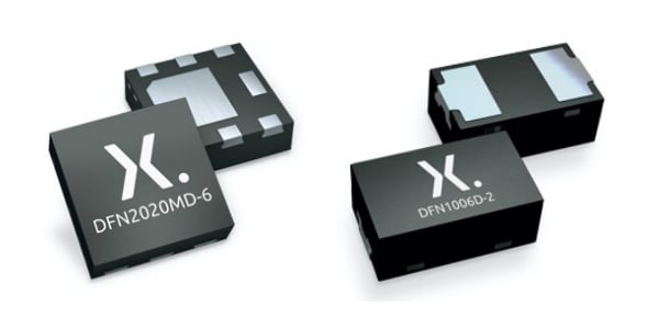
Figure 1. DFN example packages: DFN2020MD-6 (left) and DFN1006D-2 (right)
A huge variety of DFN packages are now available. The internal construction of DFN-packaged devices saves space and also leads to a reduced thermal path (Figure 2). However, QFN/DFN packages suffer a pretty significant disadvantage: the solder connection quality can only be fully inspected by costly x-ray processes, rather than automated optical inspection (AOI), because the solder connection is only underneath the plastic body of the package. The automotive industry, in particular, benefits most from the use of AOI, leading Nexperia to take a long look at solutions to this challenge.
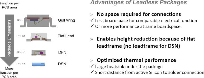
Figure 2. The advantages of leadless packages.
DFN packages are assembled in a manner similar to leaded packages except that a group of several products is molded with epoxy plastic in one shot. All QFN/DFN package lead frames consist of a copper alloy base material. Many of them are plated with a nickel-palladium-gold (NiPdAu) layer stack which is pre-applied by the lead frame supplier, guaranteeing an oxide-free surface for chip attachment, wire bonding and, on the connection pads, for wetting with solder.
Optionally, the NiPdAu layer may be additionally plated with tin. Cutting into individual devices is done after electro-galvanic tin plating. Of course, this makes tin plating of the bottom pads’ side flanks, which are exposed after sawing, impossible. The material of the side flanks of the DFN package pads is a copper alloy (lead frame base material), which may oxidize so a wetting with solder in the reflow soldering process depends on storage conditions and duration and therefore cannot be guaranteed.
Side-Wettable Flanks Guarantee Solder Wetting of Side Pads for Low I/O DFN Packages
To overcome this challenge, a solution has been developed which covers the side flanks with plated tin in the same electro-galvanic plating step as used for the bottom pads. This technique is only applicable for DFN packages with up to four pads (more if multiple pads are fused together) and the pads need to be on opposite sides of the package. Plating on all four of the pad´s side flanks on a DFN package is not possible with this method. Figures 3 and 4 show details of a DFN package with side-wettable flanks (SWF).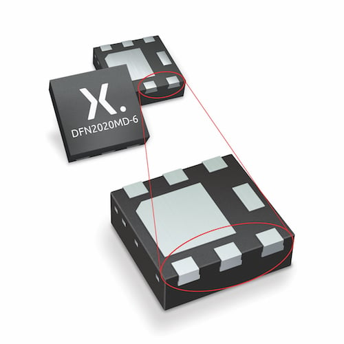
Figure 3. Detail view of side-wettable flanks in a DFN2020MD-6 package.
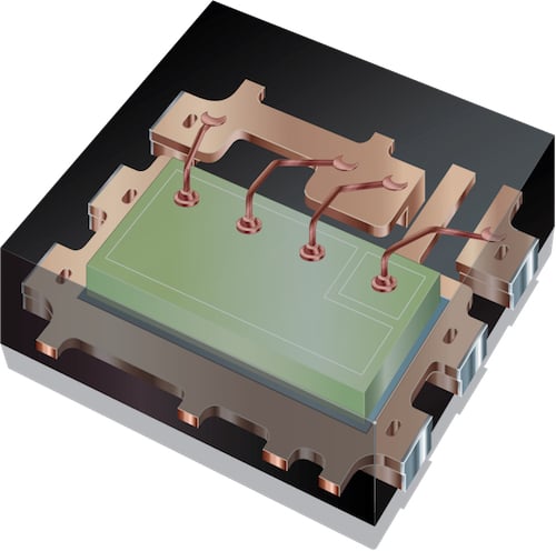
Figure 4. A cutaway view of the DFN2020MD-6 package.
The full tin-plated side-wettable flanks guarantees that the complete side pad surface is wetted with solder during the reflow soldering process. An important advantage of this process is that the plating layer on the side flank is as thick as on the bottom pads — around 10µm. This guarantees a wettable surface even after long periods of storage. Examples of the optical appearance of side flanks after soldering are shown in Figure 5 for a DFN2020-6 package with and without side-wettable flanks and in Figure 6 for the two-pad DFN1608-2 package.

Figure 5. AOI example comparison of a DFN2020-6 package with SWF versus bare copper side flanks after soldering.
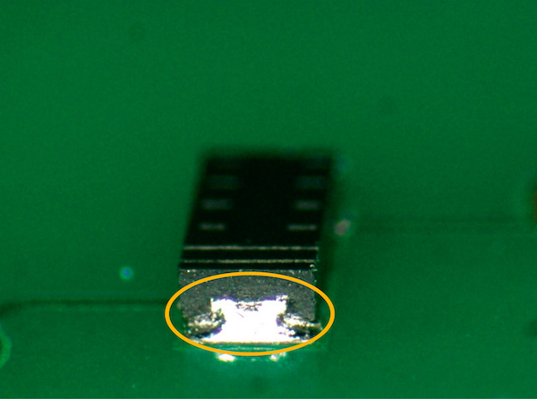
Figure 6. The appearance of side-wettable flanks (DFN1608) after soldering.
The height of the side-wettable flanks of a DFN package plated with this method depends on the lead frame thickness, but it meets the requirement of a minimum height of 100µm as raised by some automotive customers.
AOI Capability and Proof
The main purpose of the side-wettable flanks is to facilitate a reliable AOI capability for DFN packages. Thus, costly x-ray inspection can be skipped.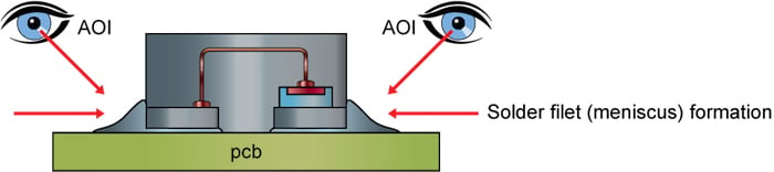
Figure 7. AOI-enabled DFN package with side-wettable flanks.
One important condition to consider is that the PCB solder pad size must be extended to be larger than the package dimension to allow space for the solder to build a meniscus or filet. The solder footprint recommendations of suppliers that offer packages with side-wettable flanks include this extra space.
To examine the suitability of Nexperia’s side-wettable flanks for AOI inspection, multiple test boards were built with solder footprints modified to accommodate the SWF package. The printed solder paste volume has been modified deliberately — on some PCB solder pads no solder was printed (see Figure 8). Working with a leading AOI equipment vendor confirmed that standard AOI techniques are able to reliably identify soldering failures using the DFN packages with SWF after reflow soldering.
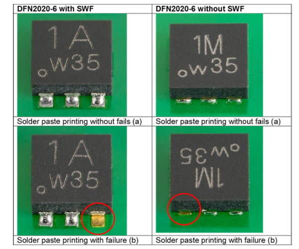
Figure 8. Example of solder failures on test board.
Additional Benefits of Low Pin Count DFN Packages with Side-Wettable Flanks
An additional benefit of DFN packages with side-wettable flanks is that the mechanical robustness of the bond to the PCB is improved when compared to devices without side-wettable flanks.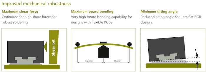
Figure 9. Board level robustness improvements of DFN packages with side-wettable flanks.
As shown in Figure 9, the shear force required to dislocate the package off the PCB is increased due to the meniscus formed after soldering. Shear force data has been collected for a DFN2020-6 package with and without side-wettable flanks. Overall, 80 samples each had been sheared on the PCB after soldering. The results show that the shear force improved by about 10% with side-wettable flanks and the standard deviation also improved (see Figure 10).
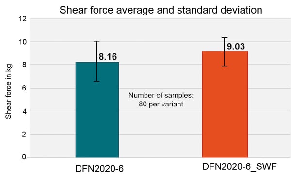
Figure 10. Shear Test on PCB for a DFN2020-6 package with and without side-wettable flanks.
Board bending tests also confirmed an increased robustness for DFN devices with side-wettable flanks — a result of additional features at the package solder pads which achieve a better anchoring to the plastic body. Summarizing the data, proves that board-bending depth for the DFN1006-2 package with SWF is up to 14mm. Some passive chip components of the same size have a bending depth often specified at 1mm.
SWF Solutions for DFN Packages with More than Six I/Os
For DFN/QFN packages with multiple I/Os (above 6) and lead-frame thicknesses of 200µm and above, one alternative is to use dimples on the side pads. Dimples are pre-etched and NiPdAu plated together with the bottom pads by the lead-frame supplier. Device separation is done at a point between two adjacent packages in the middle of the etched dimples. The wettable feature size formed by the dimples is smaller than that of the galvanic tin-plating solution previously described. Usually, packages with side-wettable flanks made in this way are delivered with NiPdAu pad plating, i.e., without additional tin-plating on the pads. Figure 11 gives an example of such a package without (left), and with (right) the dimple feature.
Figure 11. An example of multi I/O DFN/QFN package with dimples to achieve wettable flanks.
Another alternative is partial separation of the DFN packages after the molding but prior to tin plating, also known as the “saw plate saw” method. Sawing is performed to a depth that partially exposes the side flank. This means that the pads are still connected by the remaining metal part of the pad flanks ensuring that the continuity of the lead-frame is maintained for the galvanized plating process. Full device separation, with a thinner saw blade, is done after tin plating. Due to the necessary sawing tolerances, this method is — like the dimples alternative — only suitable for lead-frames greater than 200µm thick. Note that the complete height of the side flank is not covered with tin.
Electroless Tin Plating as an Alternative for Multi-I/O Packages
A technique is under investigation that would apply an electroless (immersion) tin plating process to realize the side-wettable flanks. This would allow plating of multiple pads, which could be arranged on all four sides of the DFN/QFN packages. The individual DFN/QFN package can now be fully separated prior to plating.Unlike barrel plating, the immersion process in which the packages are fixed on a carrier can achieve good layer thickness conformity. However, a disadvantage is that the growth rate of the tin is slow and the achievable tin layer thickness is less than 3µm. However, plating chemistry suppliers are starting to offer new immersion tin-plating systems that address this issue.
Nexperia offers leadless packages with the side-wettable flank option across its full standard product portfolio, including Logic and ESD protection devices, MOSFETs, diodes, and bipolar transistors. Today, ten package versions are available, and the portfolio is growing. This video shows how Nexperia’s leadless packages are meeting the requirements of the automotive industry. By featuring side-wettable flanks, they allow a visible solder joint to develop, enabling automatic optical inspection. At the same time, the packages help save space in vehicles with increasing semiconductor content due to more electronic functions while maintaining the high safety and reliability standards needed in automotive applications. For more information visit Nexperia's website.


No comments:
Post a Comment