The collection of general purpose
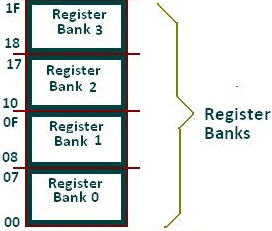
registers (R0-R7) is called as register banks, which accept one byte of
data. The bank register is a part of the RAM memory in the embedded
microcontrollers, and it is used to store the program instructions.
Each microcontroller consists of various memory banks, and each bank
register consists of a unique address for recognizing the storage
location.
Register Banks in 8051
The 8051 microcontroller
consists of four register banks, such as Bank0, Bank1, Bank2, Bank3
which are selected by the PSW (Program Status Word) register. These
register banks are present in the internal RAM memory of the 8051
microcontroller, and are used to process the data when the
microcontroller is programmed.
Switching of Register Banks
By default, the 8051 microcontroller is
powered up with register bank 0; and, by using the Program Status Word
(PSW), we can switch to other banks. The two bits of PSW are used for
switching between the register banks. These two bits are accessed by the
bit-addressable instructions SETB and CLR.
Based on the possible combinations of
RS1 and RS0 of PSW, the register bank is changed accordingly, i.e., if
RS1 and RS0 are 0, then the Bank 0 is selected. Similarly, Bank1,
2&3 are selected as per the values of RS1 and RS0.
Stack Memory Allocation in 8051 Microcontroller
The stack is an area of random access
memory (RAM) allocated to hold temporarily all the parameters of the
variables. The stack is also responsible for reminding the order in
which a function is called so that it can be returned correctly.
Whenever the function is called, the parameters and local variables
associated with it are added to the stack (PUSH). When the function
returns, the parameters and the variables are removed (“POP”) from the
stack. This is why a program’s stack size changes continuously while the
program is running.
The register used to access the stack is
called stack pointer register. The stack pointer is a small register
used to point at the stack. When we push something into the stack
memory, the stack pointer increases.
Example
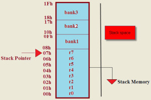
When an 8051 microcontroller power up,
the stack pointer contained value is 07, by default, as shown in the
above figure. If we perform ‘PUSH’ operation, then the stack pointer
address will be increased and shifted to another register. To avoid this
problem, before starting the program, we have to assign a different
address location to the stack pointer.
PUSH operation
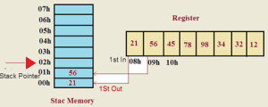
The ‘PUSH’ is used for taking the values
from any register and storing in the starting address of the stack
pointer, i.e., 00h by using ‘PUSH’ operation. And, for the next ‘PUSH’,
it increments +1, and stores the value in the next address of the stack
pointer, i.e., 01h.
PUSH operation means (First in First out)
Example: WAP in assembly language for PUSH operation
0000h
MOV 08h, #21h
MOV 09h, #56h
PUSH 00h
PUSH 01h
END
MOV 08h, #21h
MOV 09h, #56h
PUSH 00h
PUSH 01h
END
POP Operation
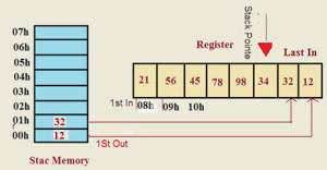
It is used for placing the values from
the stack pointer’s maximum address to any other register’s address. If
we use this ‘POP’ again, then it decrements by 1, and the value stored
in any register is given as ‘POP’.
POP operation means ‘Last in First out’.
000H
MOV 00H, #12H
MOV 01H, #32H
POP 1FH
POP 0EH
END
MOV 00H, #12H
MOV 01H, #32H
POP 1FH
POP 0EH
END
Registers of 8051 Microcontroller
If we perform any operation whether
addition or subtraction, then these operations are unable to be
performed directly in the memory, and therefore, are performed by using
the registers. There are different types of registers in 8051 microcontroller.
These registers are classified into two types based on their operations:
• General Purpose Registers
• Special Function Registers
General Purpose Registers
As we discussed earlier in this article
that there are four different bank registers with each bank having 8
addressable 8-bit registers, and only one bank register can be accessed
at a time. But, by changing the bank register’s number in the flag
register, we can access other bank registers, which have been discussed
earlier on this paper along with interrupt concept in 8051.
Special Function Registers
The special function registers including
the Accumulator, Register B, Data pointer, PCON, PSW, etc., are
designed for a predetermined purpose during manufacturing with the
address 80H to FFH, and this area cannot be used for the data or program
storage purpose. These registers can be implemented by bit address and
byte address registers.
Types of Special Function Registers
The 8051 consists of four input/output
related special function registers in which there are totally 32 I/O
lines. The special function registers control the values read from the
I/O lines and the special function registers that control the operation
of 8051. The auxiliary special function registers are not directly
connected to the 8051 – but, in fact, without these registers – the 8051
cannot operate properly. The register set of 8051 is explained below.
Register set of 8051 Microcontroller
Setting a fixed constant value in the
register is called a register set. The values are set in the registers
using instruction set. The 8051 follows CISC instructions with ‘Harvard’
architecture. The CISC stands for complex instruction set computing. Different types of instructions in the 8051 microcontroller include:
- Arithmetic Instructions
- Conditional Instructions
- Call and Jump Instructions
- Loop Instructions
- Logical Instructions
- Bullion Instructions
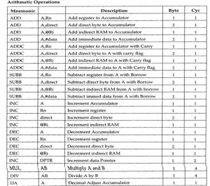
1. Arithmetic instructions
The arithmetic instructions perform several basic operations such as:
- Addition
- Subtraction
- Multiplication
- Division
Examples:
Org 0000h
MOV R0, #03H // move the value 3 is register R0//
MOV A, #05H // move the value 5 in accumulator A//
Add A, 00H // accumulator value ‘5’ with 0 and stored on accumulator//
END
b. Subtraction:
Org 0000h
MOV R0, #03H // move the value 3 is register R0//
MOV A, #05H // move the value 5 in accumulator A//
SUBB A, 03H // A=5-3 final value is 2 stored in the Accumulator A //
END
C. Multiplication:
Org 0000h
MOV R0, #03H // move the value 3 is register R0//
MOV A, #05H // move the value 5 in accumulator A//
MUL A, 03H // A=5*3 final value is 15, stored in the Accumulator A //
END
D. Division:
Org 0000h
MOV R0, #03H // move the value 3 is register R0//
MOV A, #15H // move the value 5 in accumulator A//
DIV A, 03H // A=15/3 final value is 5 stored in the Accumulator A //
END
2. Conditional Instructions
The CPU can execute the instructions
based on the condition by checking the single-bit status or byte status
is called conditional instructions such as:
To check the single-bit status in bit-addressable register
JB- jump if below
JNB- jump if not above
To check the carry bit status
JC- jump if carry flag
JNC-jump if no carry
To check the accumulator status either 0 or 1
JZ- jump if zero flag
JNZ- jump if not zero
This is all about the register set in
8051 microcontroller and their stack memory allocation. We hope this
article might have given you some essential insights about the topic
along with some very interesting programs accompanying each topic. You
can also write to us for any help in coding the microcontroller and also about the latest projects on microcontroller.




No comments:
Post a Comment