


This article will take a look at the TI’s OPA2333P which is a micro-power high-precision operational amplifier.
The OPA2333P operates from a single or dual-supply 1.8 V to 5.5 V source, has a maximum offset voltage of 10 , and incorporates a zero-drift structure which yields a maximum offset voltage drift of 0.05
The OPA2333P exhibits 1.1
noise from 0.01 Hz to 10 Hz. The device has rail-to-rail inputs and outputs and draws a quiescent current of 17
Functional Block Diagram
The functional block diagram of the OPA2333P is shown in Figure 1.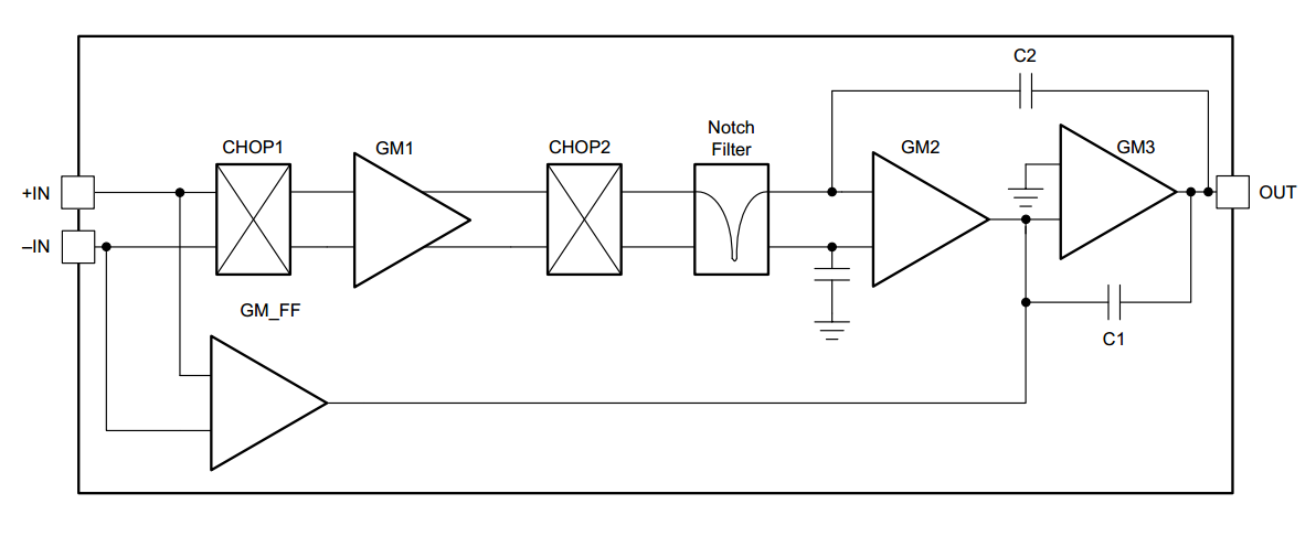
Figure 1. Image courtesy of Texas Instruments.
The device uses a proprietary offset cancellation technique which reduces the offset voltage to less than 10
and yields a near zero-drift operation.
There are four transconductance stages denoted by GM1, GM2, GM3, and GM_FF. The blocks represented by CHOP1 and CHOP2 are switching networks used to implement the mentioned auto-calibration technique. A notch filter is used to further attenuate errors. In the rest of the article, we’ll briefly look at the offset reduction technique employed in TI’s high-precision op-amps.
Offset Voltage and Drift
Input offset voltage () and input offset voltage drift over time or temperature (
For fairly high-resolution measurements, we often need an offset voltage below 1 mV. Having the amplifier offset and drift values and the application operating temperature range, we can find the worst case offset error over temperature by:
When working with micro-volt signals, amplifiers with very low offset voltage and drift are required. Some amplifiers, such as the OPA2333P, use an internal calibration mechanism to effectively reduce the offset voltage and drift. These amplifiers are often referred to as zero-drift amplifiers. The maximum offset and drift of the OPA2333P are 10
and 0.05
How a Zero-Drift Amplifier Reduces the Offset and Drift?
Let’s take a look at the technique the OPA2333P uses to perform offset cancellation. The goal is to eliminate the offset from GM1 in Figure 1. This offset voltage can be modeled as a voltage source at the input of GM1 as shown in Figures 2 and 3 below. In these figures, the switching networks represent the circuitry inside the CHOP1 and CHOP2 blocks in Figure 1.While the input is applied to +IN and -IN pins, the offset can be modeled as a voltage source at the input of GM1. This is the main feature that allows the OPA2333P to distinguish between the input signal and the offset voltage.
The offset cancellation technique incorporates two different half cycles. The first half cycle is shown in Figure 2. The voltage
is amplified by Gm1 and applied to capacitor
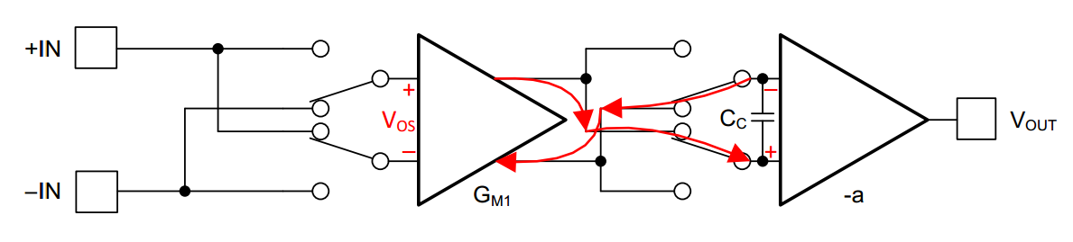
Figure 2. Image courtesy of Texas Instruments.
Now, consider the other phase as shown in Figure 3. Again the voltage
experiences the gain of Gm1 and then gets sampled on
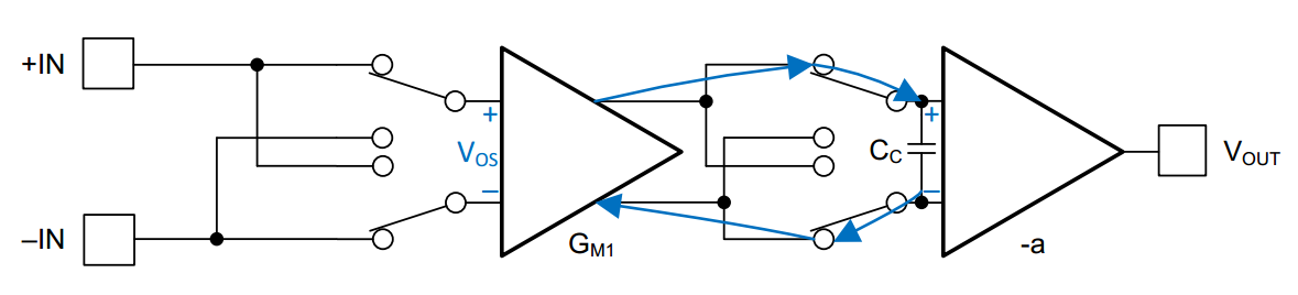
Figure 3. Image courtesy of Texas Instruments.
To prevent the input signal from being canceled out, another set of switches are placed between the input pins and Gm1. These switches are turn on and off in a way that the input signal always reaches GM2 with the same polarity. Hence, the input voltage won’t be averaged to zero by the self-correcting mechanism.
Now let’s look at some other interesting features of the device.
Low-Frequency Noise Performance
The self-correcting mechanism not only reduces the offset and drift but also suppresses the low-frequency noise of the device. Figure 4 below compares the low-frequency noise of a zero-drift amplifier with that of a traditional continuous-time amplifier.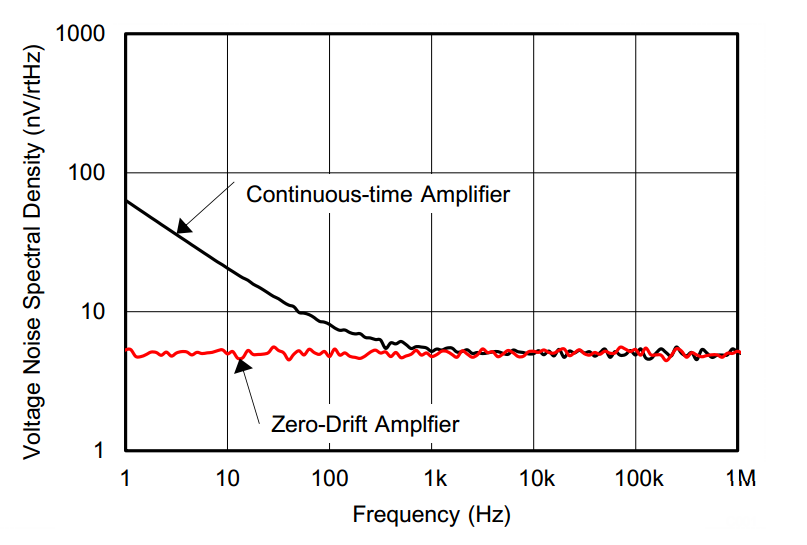
Figure 4. Image courtesy of Texas Instruments.
Generally, the low-frequency noise of zero-drift amplifiers is much lower than a continuous-time amplifier. The OPA2333P exhibits 1.1
noise from 0.01 Hz to 10 Hz.
Specified Start-Up Time
To ensure high-precision operation, the OPA2333P incorporates a specified start-up time of 500after the device is powered. After the start-up time, the device is guaranteed to achieve its specified accuracy. The test configuration and the definition of the start-up time are illustrated in Figures 5 and 6, respectively.
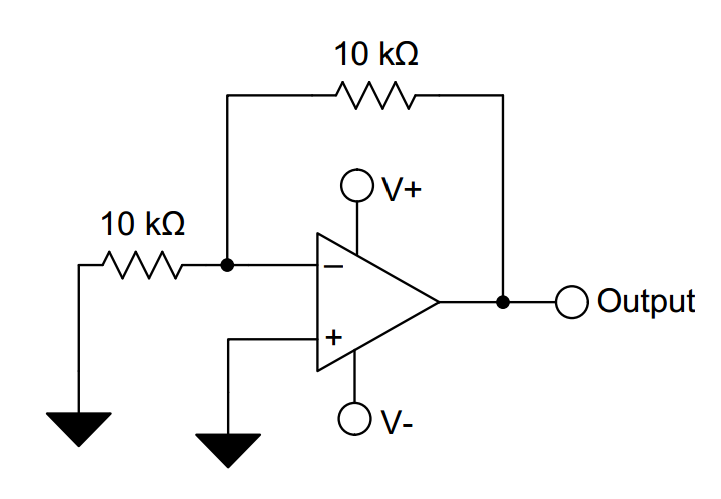
Figure 5. Image courtesy of Texas Instruments.
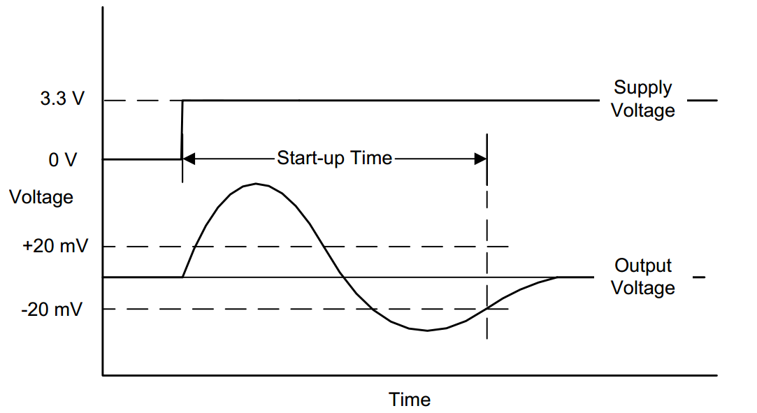
Figure 6. Image courtesy of Texas Instruments.
As shown in Figure 6, the start-up time is defined as the time duration it takes the device output to settle to within 20 mV of its nominal value after the power is connected.
Output Swing
With a single-supply operational amplifier, the output generally cannot swing to the ground potential. The output of a good single-supply operational amplifier can only get close to the ground potential. There are applications that require a voltage swing from 0 V to the positive power rail. In these applications, we can use the OPA2333P as shown in Figure 7.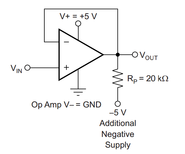
Figure 7. Image courtesy of Texas Instruments.
With this configuration, the OPA2333P output can swing to voltages even slightly below the ground potential (about -2 mV) without losing its specified accuracy. See the device datasheet for more details.
Also note that, unlike traditional rail-to-rail amplifiers that exhibit crossover distortion, the OPA2333P offers rail-to-rail voltage swing without suffering from crossover distortion associated with the traditional structures.
In this article, we looked at some of the most important features of the OPA2333P from Texas Instruments. Do you have experience with this zero-drift amplifier or other similar parts? Let us know in the comments below.


No comments:
Post a Comment