


The LT8582 is a new dual channel DC/DC converter from Linear Technology.
This highly configurable IC switches at frequencies as high as 2.5 MHz and it can be externally synchronized. It has power-good indicator pins, soft-state capability, and short-circuit protection.
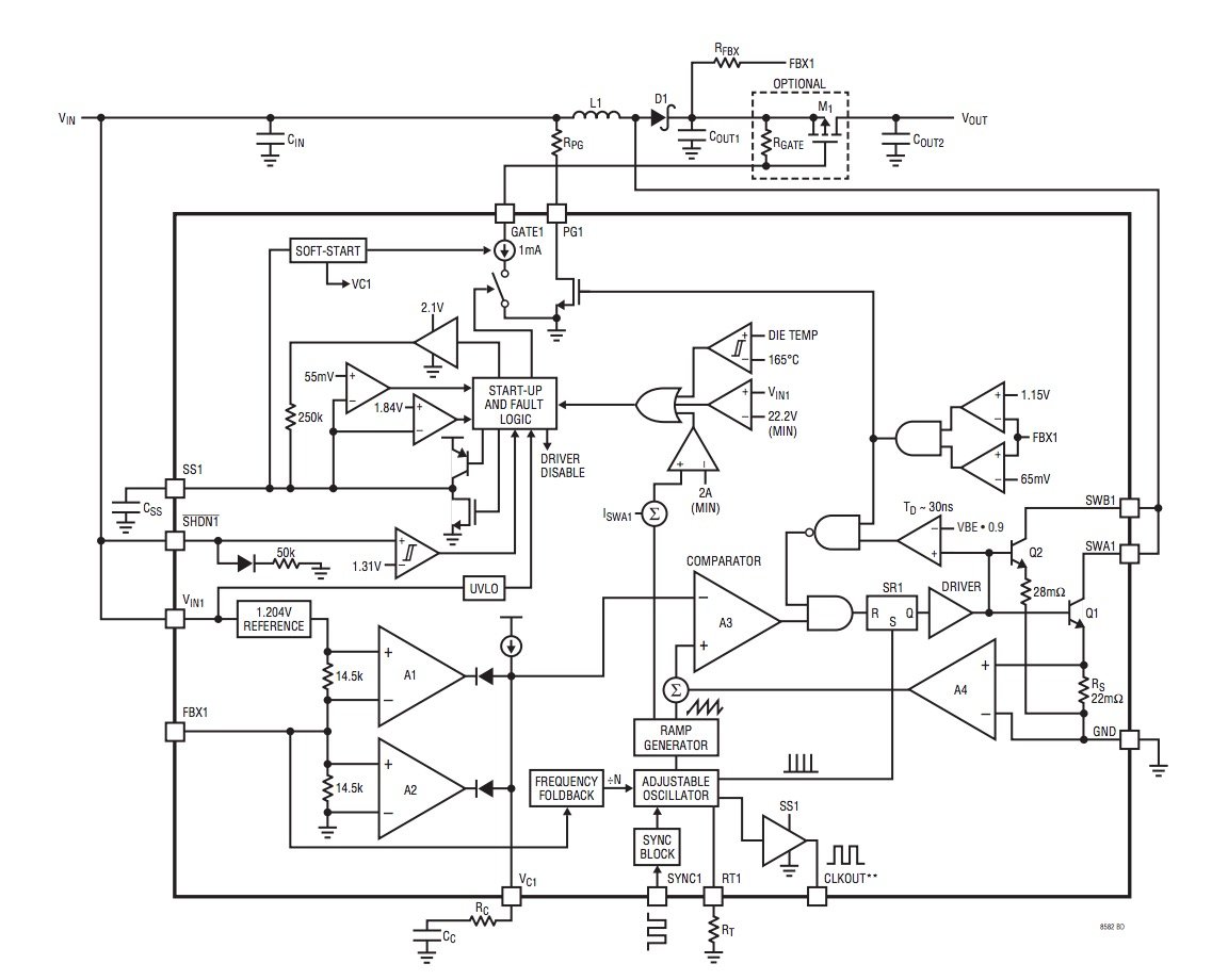
Block diagram of the LT8582, from the datasheet (PDF) Click to enlarge.
Designing with the LT8582 IC
Linear Technology has provided multiple example configurations to demonstrate how to use the device in boost converter, SEPIC, inverting, or flyback converter modes. The following schematic generates ±12 VDC at 550 mA per channel. This design is limited to relatively low current outputs to keep the device from overheating. As output current increases, proper thermal design becomes increasingly important.
Sample circuit from the LT8582 datasheet (PDF)
A few equations must be solved to calculate the values of various passive components connected to some of this ICs pins, but fortunately, Linear Tech has provided a step-by-step guide for each topology. An example is included below.
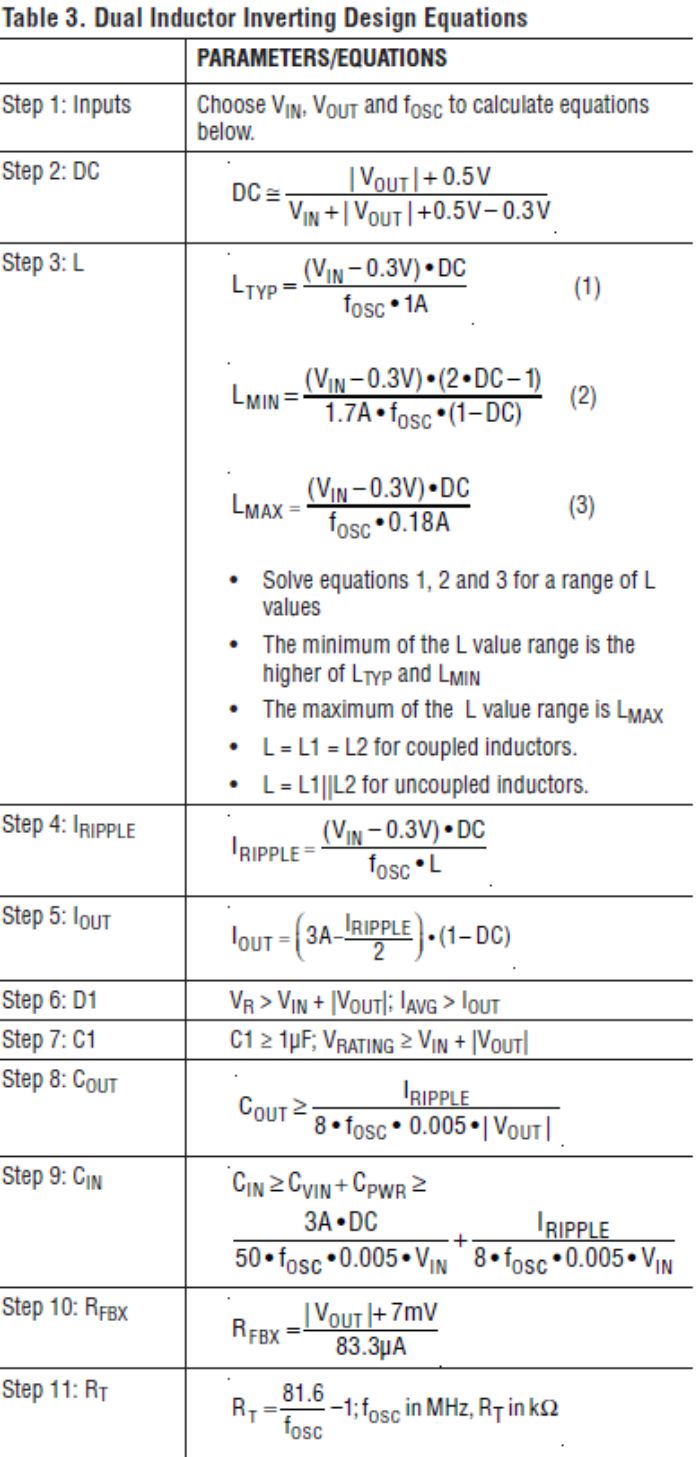
Design equations for dual inductor inverting topology
PCB Layout Considerations
The datasheet also provides two layout examples for the device. In each one, the central ground pad is connected to the ground plane with multiple vias. This is important because it allows the heat generated by the device to be transferred to other parts of the PCB.The amount of heat generated depends on the current draw of your application. Thermal engineers will likely appreciate the power dissipation calculations on page 19. Thermal energy from this device needs to be dissipated. If the die temperature exceeds 165°C, the device will stop functioning until the temperature drops below 160°C. If you intend to operate this device at high output power, you must avoid reaching temperatures anywhere near this threshold, consider active or passive cooling strategies for the IC. For example, add a heatsink or a case fan. For more information on thermal design considerations, see Thermal Design by Insight, not Hindsight (PDF) and Thermal Design Considerations for Surface Mount Layouts, both by Texas Instruments.
Shown below is the example layout on page 17. Note that it is a colorized version of what is found in the datasheet to highlight the different areas of the layout (there is no particlar significance to the colors). Vias conduct heat from the IC to the ground plane for dissipation.
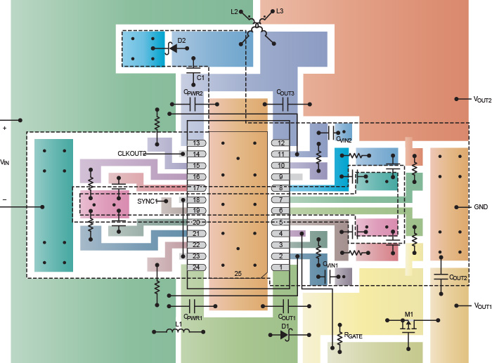
Example PCB layout from page 17 of the datasheet (PDF).
Switching circuits can be noisy, and you’ll have to be mindful of design recommendations in the datasheet to avoid creating a design that interferes with the other components on your board. That means keeping track of ground return paths and observing best design practices.Evaluation Kit Available
The DC1734A Demo Board gives engineers the opportunity to better understand a 5-10 VDC input, ±12 VDC output implementation of the LT8582. This board could come in handy if you're considering a boost or inverting design and would like to better understand and characterize the IC.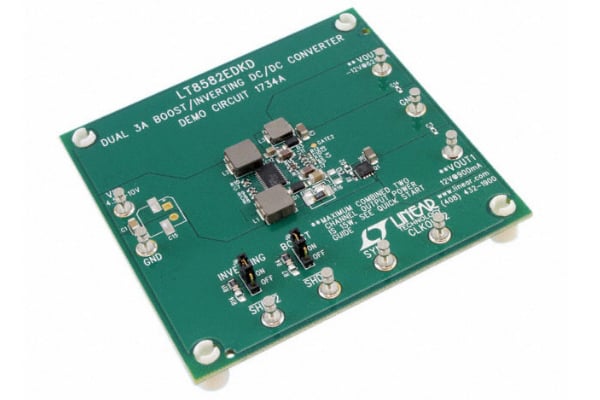
LT8582EDKD demo board. Image from Digikey
In addition to the demo board itself, Linear provides a user manual, design files, and an LTspice demo circuit (all available from the DC1734A product page).

Screen capture of an LTspice simulation for the DC1734A demo board. Click to enlarge.
This DC/DC converter IC can be configured in multiple ways. Do you have any experience using this IC in your designs? Do you have any tricks or tips to share? Feel free to leave a comment and let us know!


No comments:
Post a Comment