


In this article we’ll look at the PCB design for a low-noise ±5 V inductorless power supply.
PCB layout is always an important step in the journey from concept to a functional circuit board, but you should be particularly careful when you’re dealing with switching power-supply circuits. You want to reduce noise and improve thermal performance, and both of these objectives can be accomplished by applying standard layout techniques and following the layout recommendations in the datasheet (if there are no recommendations in the datasheet and you don’t have much experience with PCB layout, you might want to consider a different part).
Before we get started, here is the full layout (both top and bottom; all the parts are on the top):


The bottom side is used primarily as a ground plane.
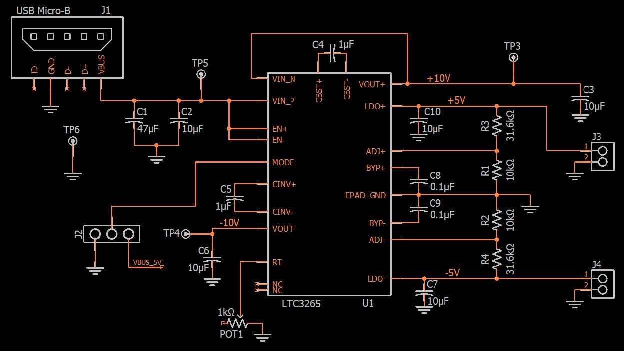
The LTC3265
The central part of my charge-pump power supply is the LTC3265 from Linear Tech/Analog Devices. It’s available in two package styles: TSSOP and DFN. TSSOPs are small but at least they have protruding leads. I assembled this board myself and if you plan to do the same, I definitely recommend the TSSOP.
As you can see, it has a thermal pad. Important: When an IC has this sort of exposed (aka thermal) pad it is typically a ground connection, but in my experience, these ICs also have at least one ground connection among the normal pins. Consequently, you may be able to get away with not connecting the exposed pad to ground (though I certainly wouldn’t recommend this).
With the LTC3265, in contrast, the exposed pad is the only ground “pin,” so you’re going to have problems if there isn’t a good connection between the exposed pad and your ground node. You can take a look at the article Stencil Design for Exposed-Pad Packages for some information on how to ensure that the exposed pad has a proper quantity of solder paste.
As I neared the end of my layout, I realized that I had no convenient way to enclose the thermal pad connection in a large copper area. Fortunately, in my case it didn’t matter much because I have no need to operate the board at high temperatures, and consequently I’m sure that I’ll get plenty of thermal relief from the six vias; these will transfer heat down to the ground plane on the bottom side of the board. If you need to maximize thermal transfer or if the bottom side of the board is not available, make sure that you leave some empty space near the two shorter sides of the LTC3265 so that you can extend the thermal-pad connection out into some large copper pours.
Inductance
My primary concern when I’m laying out a switching regulator is inductance. Switching action always leads to the presence of high frequencies; even if the switching frequency itself is rather low, the rapid on/off transitions contain high-frequency energy.More inductance means more high-frequency impedance, so inductance should be minimized. The inductance of a PCB trace is proportional to the length of the trace and inversely proportional to the width. Thus, we reduce inductance (and resistance) by making short, wide traces. You can see two examples below. The first example is my layout, and the second is the recommended layout found in the datasheet.


Here is the schematic, so that you can see which reference designators (in my layout, not the datasheet’s layout) correspond to which components.
Click to enlarge.
Manufacturing Considerations
My plan was to assemble this board using solder paste and a hot-air gun. This is a low-cost and relatively easy way to work with surface-mount components, but you have to plan ahead. If I expect to be assembling a board by hand I try to avoid anything smaller than 0805. You’ll also notice that I have a typical 0.1-inch header instead of the USB Micro-B footprint. That’s because my Micro-B connector is actually a breakout board. If you plan to assemble a PCB yourself and you need a Micro-B connection, I highly recommend this approach, at least for the prototype phase.I typically use four-layer boards because the performance is superior and routing is much simpler, but in this case, there is no need for four layers because the routing is not complicated and because the board requires only a ground plane (i.e., no power plane). Furthermore, a two-layer board allows you to use OSH Park’s Super Swift service, which in my opinion is an excellent option for low-cost, quick-turn PCB fabrication.
I recently learned about the existence of bismuth-based solder. This type of solder is great for prototyping because it melts at a lower temperature—in the case of the product that I used, 138°C, compared to ~183°C for leaded solder or ~220°C for typical lead-free solder. I used bismuth-based solder to assemble the inductorless bipolar power supply, and all I can say is that I will never go back to the other stuff. The low melting point allowed me to assemble the board with less thermal stress on the components (and less psychological stress for myself), and rework was easier and faster (and again, less stressful).
Conclusion
I’ve already assembled and tested this charge-pump power supply, and I’m very pleased with the results (which will be published in an upcoming project article). It’s a straightforward and compact solution; my PCB was only ~1.3 square inches. If you think of this circuit as a subsystem that would be incorporated into a larger PCB, and if you eliminate the prototype-only components, it becomes even smaller because you could eliminate J1, C1, POT1, J2, J3, J4, and TP3–5. This will definitely become my go-to solution whenever I need symmetric rails for low-current analog or mixed-signal circuitry.


No comments:
Post a Comment