


The growing use of wireless data
is driving demand for communication systems that can transmit more data
with greater energy efficiency, in order to both cut operating costs
and, in mobile devices, to increase battery life.
It’s
especially challenging for a transmitter’s power amplifier (PA) to meet
both demands at once since it needs to achieve high average efficiency
at the same time as coping with the high peak-to-average-power ratios
(PAR) of the complex wideband modulation schemes used by the latest
cellular standards.The average efficiency of the PA is mainly determined by the efficiency of the driver and the end stage.
Ampleon built a two-stage GaN RF PA MMIC that uses a GaN transistor operating at low voltage as a driver. This increases the average efficiency of the overall PA by both decreasing the power consumption of the driver and eliminating the need for inter-stage matching between it and the end stage.
The end stage of the MMIC is terminated with a quasi load-insensitive (QLI) class-E load network to achieve high efficiency, despite the large output power variation caused by load modulation. This load network is built in a standard RF package, using bond-wire and package-lead capacitance.
Load-pull measurements show that the overall power efficiency of the PA remains greater than 70% despite a wide range of load modulations, such as an 8dB variation in output power. This sustained efficiency makes the MMIC useful for PA architectures that rely upon load modulation, such as the Doherty and Outphasing approaches.
To create a demonstration PCB, Ampleon uses their MMIC. The linear gain of this system measured around 27dB, with a maximum efficiency of 76% at an output power of 35.4dBm at 2.14 GHz. The supply voltages of the driver and the end stage are 5.5V and 25V, respectively. A WCDMA signal was applied with a vector-switched generalized memory polynomial digital pre-distortion (VS-GMP DPD) algorithm to our demo set-up, and achieved a –52.4dBc adjacent channel leakage ratio at 29.4dBm average output power.
Circuit Architecture
The schematics of the conventional and the new low-voltage driver RF PA line-ups are shown at left and right of Figure 1, respectively.
Figure 1: Left: the conventional high-voltage driver RF PA. Right: the low-voltage driver RF PA.
The conventional approach uses the same supply voltage for both the driver and the end stage, which means the overall PA needs a matching network between its driver and end stage. Using a low supply voltage on the driver reduces its output impedance enough that the overall PA does not need such a matching network, which reduces power losses. The low driver supply voltage also reduces the driver’s power consumption, which improves the overall efficiency. Getting rid of the inter-stage matching network also cuts the size of the MMIC, so reducing costs.
Fig 2 compares the overall efficiency of the conventional high-voltage and the new low-voltage driver RF PA topologies in a simulation. Although the simulated drain efficiencies (DE) are almost the same for high-voltage and low-voltage cases, there is a significant difference in power added efficiency (PAE).

Figure 2. Simulated comparisons of drain efficiency (top) and power added efficiency (below) for the twp driver architectures when the PA is operating at 2.14 GHz.
The Two-Stage GaN HEMT MMIC Design
The MMIC was built as a two-stage amplifier using Fraunhofer’s IAF 0.25mm GaN HEMT technology on a multi-project wafer. The driver stage and the end stage have 0.488mm and 2.4mm total gate widths, respectively. The end-stage transistor and the driver transistor are integrated on a die with the AC-coupling capacitor and gate bias resistors, as shown in Figure 3.The In-Package Quasi Load-Insensitive Class E Load Network
The end stage of the MMIC is terminated with a QLI Class E load network, to ensure high efficiency despite a wide variation in output powers caused by load modulation.The MMIC and its QLI Class-E load network were assembled in a SOT1112A standard Ampleon air-cavity ceramic package, and used bond-wire and package lead capacitances to produce two key reactive elements: L1 at 4.9nH and C1 at 1.5pF.
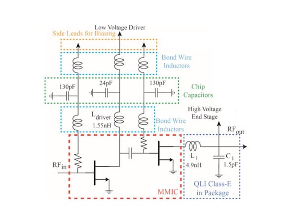
Figure 3. A schematic of the assembled MMIC and its load network.
Figure 4 shows the efficiency of the packaged MMIC under load-pull measurements, demonstrating that the packaged MMIC can sustain its high efficiency under a large load variation.

Figure 4. Drain efficiency and power added efficiency of the low voltage driver MMIC during pulsed load-pull measurements at 2.14 GHz.
Building a Demo Board and Measuring it with a Modulated Signal
To further prove the value of the low-voltage driver approach Ampleon designed a PCB to mount the MMIC on, and tuned its output load to match the impedance at which the MMIC alone achieved its maximum efficiency under the load-pull measurements referenced above.The PCB was prepared using Rogers RO4350B as the substrate and is shown in Figure 5 with its biasing and matching components.

Figure 5. Components and their values on the PCB, with inset, the mounted PA.
Figure 6 shows the drain efficiency, power-added efficiency and gain of the mounted PA, measured with a 2.14GHz continuous-wave signal. The peak PAE is 76%. The driver power consumption is so low that the difference between the drain and the power-added efficiency is negligible at low and high output power levels. The measured small signal gain is around 27dB at 2.14GHz.

Figure 6. Measured gain, drain efficiency (black line) and power added efficiency (red squares) of the final circuit.
Conclusion
Using low-voltage driver circuits can help achieve high overall PA efficiency in 0.25μm GaN HEMT technology. Our measurements show that a low-voltage driver MMIC, assembled in an RF package with a QLI Class- E load network, can create a PA whose efficiency remains greater than 70% in the presence of an 8dB output power variation. This makes the MMIC a good candidate for use in PA architectures that rely upon load modulation, such as the Doherty and Outphasing approaches.This article was co-written by Mustafa Acar, Osman Ceylan, Felicia Kiebler, Sergio Pires, and Stephan Maroldt.


No comments:
Post a Comment