


In this teardown, we cut into a Depstech endoscope to see what we can find.
First Impressions
Before beginning the tear of Depstech's HD WiFi Inspection Camera, I tested it (played with it) a bit to see how well it worked. In a word: Wow!This is an amazing piece of inexpensive technology. For less than $40 (at the time of writing this article), this is an easy-to-use and waterproof Wi-Fi endoscope that works seemingly flawlessly. Connecting it to my iPhone 5s was a snap as the free app looks to be bug-free. Take this information with a grain of salt because I only tested the camera for about 5 minutes before tearing it open, so by no means did I put this camera (and its app) through the ringer of exhaustive testing.
The video link below shows my very brief testing of this endoscope, including a water test. Note that the camera's video footage can be seen on my iPhone's screen. During the mere 5 minutes that I tested the camera, I did notice—as called out in the user manual—that it got a little warm/hot due to the LEDs being set to their maximum setting.
The image below shows everything that was included in the shipping box.

Everything included in the packaging box.
Specifications
The following specs were taken from Depstech's website:- Resolution: 1280×720, 640×480, 320×240
- Camera diameter: 8.4mm
- Waterproof: IP67
- Wi-Fi transmission distance: 15 meters
- Battery capacity: 600mAh
- Focal distance: 3CM-6CM
- Power supply: DC 5V
The images below show various views of the Wi-Fi box as well as the camera accessories.

Multiple views of the Wi-Fi box, including its label.

Accessory pieces. Image courtesy of Depstech.com.
Okay, enough playin' around...let's tear this thing open!!
Opening the Wi-Fi Box
I began the teardown process by opening the Wi-Fi box. This plastic box is held together with four small Phillips-head screws. Once the lid is removed, a rather small PCB becomes visible, as well as the rechargeable lithium-ion battery (see image below).
Inside the Wi-Fi box is a single PCB and the rechargeable lithium-ion battery.
Although the functionality of the camera seemed to work perfectly, the assembly quality of this box seems to be less than ideal. In the image above, note the missing screw and the low-quality tape attached to the battery (presumably to prevent it from flopping around). Also notice the standoffs that are cracked or broken.
The PCB Inside the Wi-Fi Box
PCB "Front" Side
The image below shows one side (let's call this side the front side) of the PCB. And although the ICs are clearly part marked, it was not always possible to find their datasheets.
Major components on the PCB's front side.
The list below calls out the major electrical components and their part markings; included, when possible, are links to datasheets or additional information.
- Crystal: 40.0MHz. Part marking: 40.0 SJJ.
- Voltage regulators:
- Part marking: A17K (qty 2)
- Part marking: B6287
- Schottky rectifier. Part marking: SS14
- Processor/Wi-Fi controller: Ralink RT5350
- Regulator (either voltage or constant-current): Part marking: S2QA
One final observation when viewing this side of the PCB: the hot glue, applied to the five wires that are soldered to the PCB, serves as strain relief for those wires. Although this approach is better than not having any strain relief and it's most likely a very inexpensive solution, this method is not ideal.
PCB "Back" Side
Let's take a look at the PCB's back side. Again, the major components have been noted in the image below:
Major components on the PCB's back side.
The components found on the back side of the PCB include:
- NPN transistor: Part marking: 1AM
- Memory (Flash): Part marking: Winbond 25Q32JVSIQ
- Memory (DRAM): Part marking: ESMT M12L2561616A
- Unknown IC: Part marking: 58b8
- P-Channel MOSFET: Part marking: A1sHB
- Diode: Part marking: MDD K14
As can be seen in the image below, the lithium-ion battery has protection circuitry attached to a small PCB of which is soldered to the leads of the battery.

Major components on the PCB's back side.
The components on this PCB include:
- Unknown IC (perhaps a voltage regulator): Part marking: G3JU
- Dual FET: Part marking: 8205A
The Camera Probe
Let's now turn our attention to the camera probe. As noted in the user manual, this camera has an IP67 rating, which means that it can withstand some water. To quote the user manual: "The camera probe is only IP67 waterproof which means it can only do underwater inspections for no deep than 1meter and no more than several minutes." Kudos for being IP67 rated. Unfortunately, this means that the probe was rather difficult to open-up for inspection.The camera probe housing is made from metal. After observing that it had multiple pieces screwed together, I attempted—and failed—to unscrew these pieces. The video link below shows my futile efforts of using vise-grips to unscrew the two pieces. Regrettably, this approach only marred the metal enclosure.
My next attempt to see inside the camera probe—and to penetrate its IP67 protections—was to fire up the Dremel. For the record, I decided to use this mini grinder only as a last resort. Using a Dremel will most definitely result in the destruction of a device, and I always feel a bit guilty when destroying a perfectly working device... especially one as cool as this wireless endoscope.
The video below shows me cutting (literally) into the camera's probe. Although you can't see my head in the video, I am wearing hearing protection and a safety face shield.
Success! ...sort of.
Whenever cutting into an enclosure, one always runs the risk of unintentionally damaging unseen components. This was the case here, and, of course, the main IC inside the enclosure is what was damaged. As can be seen in the image below, I managed to grind off the image sensor processor's part marking.
Nonetheless, the PCB—actually it's a flex circuit—that lives inside the camera probe's enclosure looks mighty impressive, yet simple.

Camera probe's PCB (front side)—it's a flex circuit.
The back side of the PCB contains two voltage regulators and some potting/epoxy:
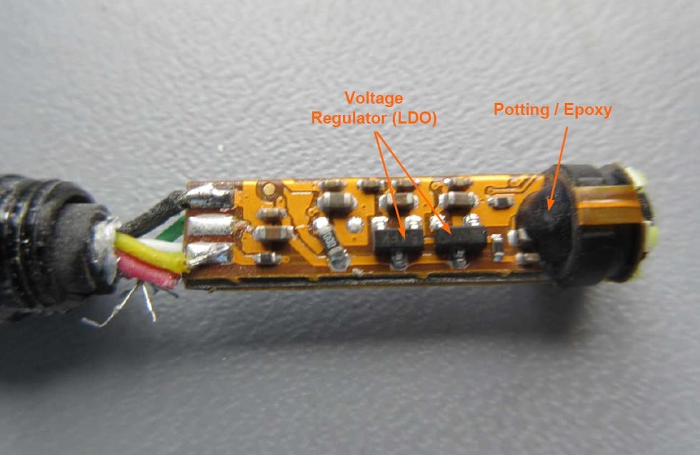
Camera probe's PCB (back side).
Also integrated on the flex circuit is an LED ring consisting of six LEDs. This ring is attached to the camera's lens, which simply screws into the camera's module housing (see image below).

Camera lens and LEDs.
When looking down/inside the camera module, the camera's image sensor can be seen. This sensor is also attached/soldered to the flex circuit. The image below shows this sensor through a microscope.

Camera's image sensor mounted on the flex circuit.
Unfolding the Flex Circuit
The final tear down step was the unfolding of the flex circuit. After desoldering the wires and cutting off the glued-on plastic image sensor housing, it was quite easy to simply unfold the PCB/flex circuit.
The flex circuit unfolded.
The metal pieces on the back side (which are glue-on) serve as stiffeners for this flex circuit.


No comments:
Post a Comment