


Communication plays an essential role in
the embedded system designing. Without going to the protocols, the
peripheral expansion is highly complex and high-power consuming. The embedded system basically uses serial communication to communicate with the peripherals.
There are many serial communication protocols, such as UART, CAN, USB, I2C and SPI communication. The serial communication protocol’s characteristics include high speed and low data loss. It makes system-level designing easier, and ensures reliable data transfer.
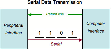
Serial Data Communication
Electrically-coded information is called
a serial data, which is transmitted bit by bit from one device to
another through a set of protocols. In the embedded system, control
sensors and actuators data is received or transmitted to the controller
devices such as microcontrollers so that the data is further analyzed
and processed. As the microcontrollers work with the digital data, the
information from the analog sensors,
actuators and other peripherals is converted into one byte (8-bit)
binary word prior to being transmitted to the microcontroller.
Serial Data Communication
This serial data is transmitted with
respect to certain clock pulse. The data transmission rate is referred
to as the baud rate. The number of data bits that can be transmitted per
second is called as baud rate. Suppose the data is of 12 bytes, then
each byte is converted into 8bits so that the total size of the data
transmission is about 96bits/sec of the data (12bytes*8 bits per byte).
If the data can be transmitted once every second, the baud rates are
around 96bits/sec or 96 baud. The display screen refreshes the data
value once every second.
Serial Peripheral Interface Basics
The SPI communication stands for serial peripheral interface communication protocol,
which was developed by the Motorola in 1972. SPI interface is available
on popular communication controllers such as PIC, AVR, and ARM controller,
etc. It has synchronous serial communication data link that operates in
full duplex, which means the data signals carry on both the directions
simultaneously.
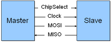
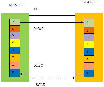
SPI protocol consists of four wires such
as MISO, MOSI, CLK, SS used for master/slave communication. The master
is a microcontroller, and the slaves are other peripherals like sensors,
GSM modem
and GPS modem, etc. The multiple slaves are interfaced to the master
through a SPI serial bus. The SPI protocol does not support the
Multi-master communication and it is used for a short distance within a
circuit board.
Serial Peripheral Interface Basics
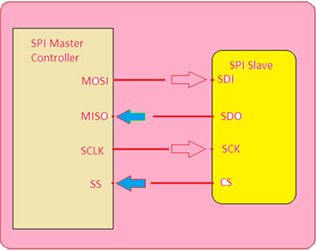
SPI Lines
MISO (Master in Slave out): The MISO line is configured as an input in a master device and as an output in a slave device.
MOSI (Master out Slave in):
The MOSI is a line configured as an output in a master device and as an
input in a slave device wherein it is used to synchronize the data
movement.
SCK (serial clock):
This signal is always driven by the master for synchronous data transfer
between the master and the slave. It is used to synchronize the data
movement both in and out through the MOSI and MISO lines.
SS (Slave Select) and CS (Chip Select):
This signal is driven by the master to select individual
slaves/Peripheral devices. It is an input line used to select the slave
devices.
Master Slave Communication with SPI Serial Bus
Single Master and Single Slave SPI Implementation
Here, the communication is always
initiated by the master. The master device first configures the clock
frequency which is less than or equal to the maximum frequency that the
slave device supports. The master then selects the desired slave for
communication by dragging the chip select line (SS) of that particular
slave device to go low state and active. The master generates the
information on to the MOSI line that carries the data from master to
slave.
Master Slave Communication
Single Master and Multiple Slave Implementations
This is a multiple slave configuration
with one master and multiple slaves through the SPI serial bus. The
multiple slaves are connected in parallel to the master device with the
SPI serial bus. Here, all the clock lines and data lines are connected
together, but the chip select pin from each slave device must be
connected to a separate slave select pin on the maser device.
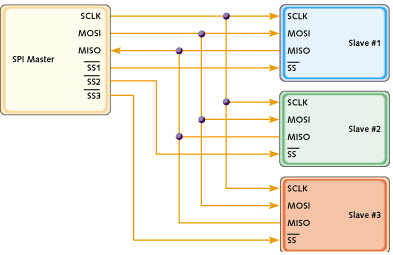
Single Master and multiple slaves
In this process, the control of each
slave device is performed by a chip select line (SS). The chip select
pin goes low to activate the slave device and goes high to disable the
slave device.
The data transfer is organized by using
the shift registers at both master and slave devices with a given word
size of about 8-bit and 16-bit, respectively. Both the devices are
connected in a ring form so that the maser shift register value is
transmitted through the MOSI line, and then the slave shifts data in its
shift register. The data is usually shifted out with the MSB first and
shifting new LSB into the same register.
Data Transfer between Master and Slave
Significance of Clock Polarity and Phase
Generally the transmission and reception
of data is performed with respect to the clock pulses at rising edges
and falling edges. The Advanced microcontrollers have two frequencies:
internal frequency and external frequency. SPI peripherals could be
added by sharing the MISO, MOSI and SCLK lines. The peripherals are of
different types or speeds like ADC, DAC, etc. So we need to change the
SPCR settings between the transfers to different peripherals.
SPCR register
The SPI bus operates in one of the 4
different transfer modes with a clock polarity (CPOL) and clock phase
(CPHA) which defines a clock format to be used. The clock polarity and
the phase clock rates depend on which peripheral device you are trying
to communicate with the master.
CPHA=0, CPOL=0: The first bit starts as a lower signal – the data is sampled at rising edge and the data changes on falling edge.
CPHA=0, CPOL=0: The first bit starts as a lower signal – the data is sampled at rising edge and the data changes on falling edge.
CPHA=0, CPOL=1: The first bit starts
with a lower clock – the data is sampled at falling edge and the data
changes on rising edge.
CPHA=1, CPOL=0: The first bit starts
with a higher clock – the data is sampled at falling edge and the data
changes on rising edge.
CPHA=1, CPOL=1: The first bit starts
with a higher clock – the data is sampled at rising edge, and the data
changes on falling edge.
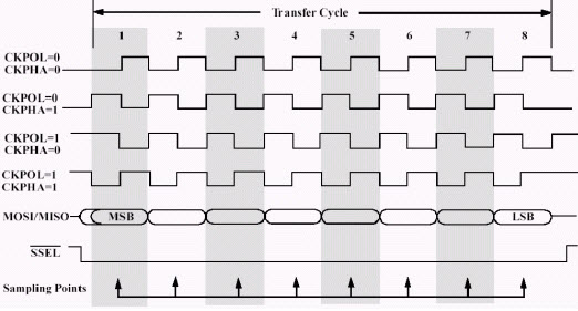
SPI Bus timings
SPI Communication Protocol
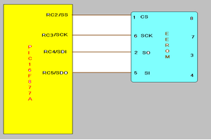
Many microcontrollers have inbuilt SPI
protocols that handle all of the sending and receiving data. Any of the
data mode operations (R/W) is controlled by a control and status
registers of the SPI Protocol. Here, you can observe the EEPROM
interface to the PIC16f877a microcontroller through the SPI protocol.
Here, 25LC104 EEROM is a 131072 bytes memory wherein the microcontroller transfers two bytes of data to the EEROM memory through a SPI serial bus. The program for this interfacing is given below.
Master to Slave communication through SPI
serial bus
#include
Sbit SS=RC^2;
Sbit SCK=RC^3;
Sbit SDI=RC^4;
Sbit SDO=RC^5;
Void initialize EEROM();
Void main()
{
SSPSPAT=0x00;
SSPCON=0x31;
SMP=0;
SCK=0;
SDO=0;
SS=1;
EE_adress=0x00;
SPI_write( 0x80);
SPI_write(1234);
SS=0;
}
Sbit SS=RC^2;
Sbit SCK=RC^3;
Sbit SDI=RC^4;
Sbit SDO=RC^5;
Void initialize EEROM();
Void main()
{
SSPSPAT=0x00;
SSPCON=0x31;
SMP=0;
SCK=0;
SDO=0;
SS=1;
EE_adress=0x00;
SPI_write( 0x80);
SPI_write(1234);
SS=0;
}
Advantages of SPI Protocol
- It is a full duplex communication.
- It is high-speed data bus 10MHzs.
- It is not limited to 8bits while transferring
- Hardware interfacing is simple through SPI.
- Slave uses a master clock and doesn’t need precious oscillators.
This is all about the SPI communications and its interfacing with a microcontroller.
We appreciate your keen interest and attention for this article and
hence anticipate your viewpoint on this article. Furthermore, for any
interfacing coding and assistance, you can ask us by commenting below.


No comments:
Post a Comment