A microcontroller is a small computer on
a single IC that integrates all the features that are found in the
microprocessor. In order to serve different applications, it has a high
concentration of on chip facilities such as RAM, ROM, I/O ports, timers,
serial port, clock circuit and interrupts. Microcontrollers are used in
various automatically controlled devices such as remote controls,
automobile engine control systems, medical devices, power tools, office
machines, toys, and other embedded systems. Therefore, this article gives an overview of the pin diagram of 8051 microcontroller with explanation and also 8051 based project ideas.
In case of microprocessor, we have to
interface additional circuitry externally, such as RAM, ROM, I/O ports,
timers, serial port, clock circuit, and other external peripherals,
whereas in the microcontroller, all these peripherals are in built. Let
us look in brief about the pin diagram of the 8051 microcontroller.
Microcontroller Pins Working
8051 microcontrollers have four I/O
ports where in each port contains 8 pins that can be configured as
inputs or outputs. The Pin configuration – whether it to be configured
as an I/P (1) or an O/P (0), depends on its logic state. In order to
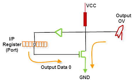
configure a microcontroller pin as an output, it is necessary to apply a
logic zero (0) to the suitable I/O port bits. In this case, the voltage
level at the appropriate pin will be 0.
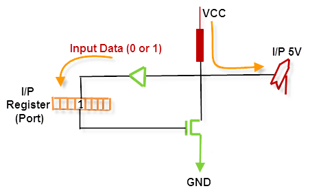
Similarly, in order to configure a
microcontroller pin as an input, it is necessary to apply a logic one
(1) to the suitable port. In this case, the voltage level on the
appropriate pin will be 5V. This may seem confusing, It all becomes
clear after studying simple electronic circuits connected to an I/O pin.
Input/Output (I/O) Pin
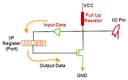
The below figure shows a
simplified schematic of all circuits within the microcontroller, which
is connected to one of its pins. It states to all the pins except those
of the P0 port that do not have pull-up resistors built-in.
Output pin
A logic 0 is applied to a bit of the
register P, then the output FE transistor is turned on,
therefore connects the appropriate pin to ground.
Input pin
A logic 1 is applied to a bit of the P register. The output field effect transistor
is turned off, and the appropriate pin remains connected to the power
supply voltage, over a pull-up resistor of high resistance.
Pin Diagram of 8051 Microcontroller
8051 microcontroller
families (89C51, 8751, DS89C4xO, 89C52) come in different packages
like quad-flat package, leadless chip carrier and dual-in-line package.
These all packages consist of 40 pins which are dedicated to several
functions such as I/O, address, RD, WR, data and interrupts. But, some
companies offer a 20-pin version of the microcontrollers
for less demanding applications by reducing the number of I/O ports.
Nevertheless, a vast majority of developers use the 40-pin chip.
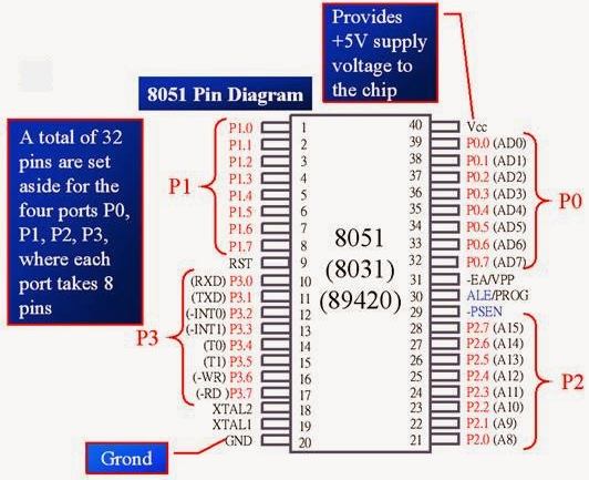
The pin diagram of 8051 microcontroller
consists of 40 pins as shown below. A total of 32 pins are set away into
four Ports such as P0, P1, P2 and P3. Where, each port contains 8 pins.
Therefore, the microcontroller 8051’s pin diagram and explanation is
given below.
- Port1 (Pin1 to Pin8): Port1 includes pin1.0 to pin1.7 and these pins can be configured as input or output pins.
- Pin 9 (RST): Reset pin is used to Reset 8051 Microcontroller by giving a positive pulse to this Pin.
- Port3 (Pin 10 to 17): The Port3 Pins are similar to port1 pins and can be used as universal Input or output pins. These pins dual-function Pins and the function of each Pin is given as:
- Pin 10 (RXD): RXD pin is a Serial Asynchronous Communication Input or Serial synchronous Communication Output.
- Pin 11 (TXD): Serial Asynchronous Communication Output or Serial Synchronous Communication clock Output.
- Pin 12 (INT0): Input of Interrupt 0
- Pin 13 (INT1): Input of Interrupt 1
- Pin 14 (T0): Input of Counter 0 clock
- Pin 15 (T1): Input of Counter 1 clock
- Pin 16 (WR): Writing Signal to write content on external RAM.
- Pin 17 (RD): Reading Signal to read contents of external RAM.
- Pin 18 and 19 (XTAL2, XTAL1): X2 and X1 pins are input output pins for the oscillator. These pins are used to connect an internal oscillator to the microcontroller.
- Pin 20 (GND): Pin 20 is a ground pin.
- Port2 (Pin 21 to Pin28): Port2 includes pin21 to pin28 which can be configured as Input Output Pins. But, this is only possible when we don’t use any external memory. If we use external memory, then these pins will work as high order address bus (A8 to A15).
- Pin 29 (PSEN): This pin is used to enable external program memory. If we use an external ROM for storing the program, then logic 0 appears on it, which indicates Micro controller to read data from the memory.
- Pin 30 (ALE): Address Latch Enable pin is an active high-output signal. If we use multiple memory chips, then this pin is used to distinguish between them. This Pin also gives program pulse input during programming of EPROM.
- Pin 31 (EA): If we have to use multiple memories then the application of logic 1 to this pin instructs the Microcontroller to read data from both memories: first internal and then external.
- Port 0 (Pin 32 to 39): Similar to the port 2 and 3 pins, these pins can be used as input output pins when we don’t use any external memory. When ALE or Pin 30 is at 1, then this port is used as data bus: when the ALE pin is at 0, then this port is used as a lower order address bus (A0 to A7)
- Pin40 (VCC): This VCC pin is used for power supply.
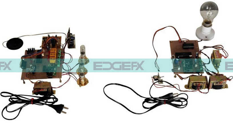
There are many applications of 8051 microcontroller. So, 8051 microcontroller projects
are of great for engineering final year. Therefore, you can refer any
one of the below listed projects to understand the 8051
microcontroller’s pins operations practically.
- Bidirectional Rotation of Single Phase Induction Motor without Run Capacitor
- Over Voltage- Under Voltage Protection
- Wireless Rash Driving Detection
- Arduino based Home Automation
- Android based Remotely Programmable Sequential Load Operation
- War Field Spying Robot with Night Vision Wireless Camera by Android Applications
- Remote Operated Domestic Appliances Control by Android Application
- Density Based Auto Traffic Signal Control with Android Based Remote Override
- Four Quadrant Operation of DC Motor Remotely Controlled by Android Application
- Remote Alignment of 3D Dish Positioning by Android Application
- Password based Remote Controlled Door Opening by Android Application
- Voice Controlled Robotic Vehicle with Long Distance Speech Recognition
- XBEE Based Remote Monitoring of 3 Parameters on Transformer / Generator Health with Voice Announcement and Wireless PC Interface
- Railway Level Crossing Gate Operation Remotely by Android
- Home Automation by Android Application Based Remote Control
- Wireless Power Transfer in 3D Space
- Density Based Traffic Signal with Remote Override in Emergency
- XBEE Based Remote Monitoring of 3 Parameters on Transformer / Generator Health
- Self-Switching Power Supply
- RFID Based Paid Car Parking
- Led Based Automatic Emergency Light
- Contactless Liquid Level Controller
This is about the microcontroller pins working priciples with the real-time 8051 microcontroller based project ideas. Furthermore, any queries regarding this article or latest electronics projects, contact us by commenting in the comment section below.
Photo Credits:
Pin Diagram of 8051 Microcontroller blogspot8051 Microcontrollercotsjournalonline

No comments:
Post a Comment